MSc Physics物理學碩士 Graduate - NCUE Taiwan
Mudassar Iqbal|
MSc Physics物理學碩士 graduate focused on thin-film process development, wet etch, LC photonic devices, optical metrology, and fabrication troubleshooting for semiconductor display roles.
5+Research Projects
3 yearsResearch Experience
Mudassar Iqbal
Process Engineer

Autobiography
About Me
& My Journey關於我
與我的經歷
Academic background
Physics training with a graduate focus on photonics, semiconductor technology, thin-film processes, and optics.
The University of Lahore拉合爾大學
2018 - 2022Bachelor of Science in Physics物理學學士
PakistanTechnical strengths專業技術
Relevant Skills相關專業技能
A multidisciplinary engineering skill set combining semiconductor process development, thin-film fabrication, optical device engineering, characterization, and data-driven process optimization.
01
Thin-Film Process製程ing & Semiconductor Materials
02
Photolithography & Microfabrication
03
Process製程 Control & Wet Process製程ing
04
Device Development & Experimental Engineering
05
Process製程 Optimization & Data Analytics
06
Deep Learning & Computational Modeling
Changhua, Taiwan台灣彰化01
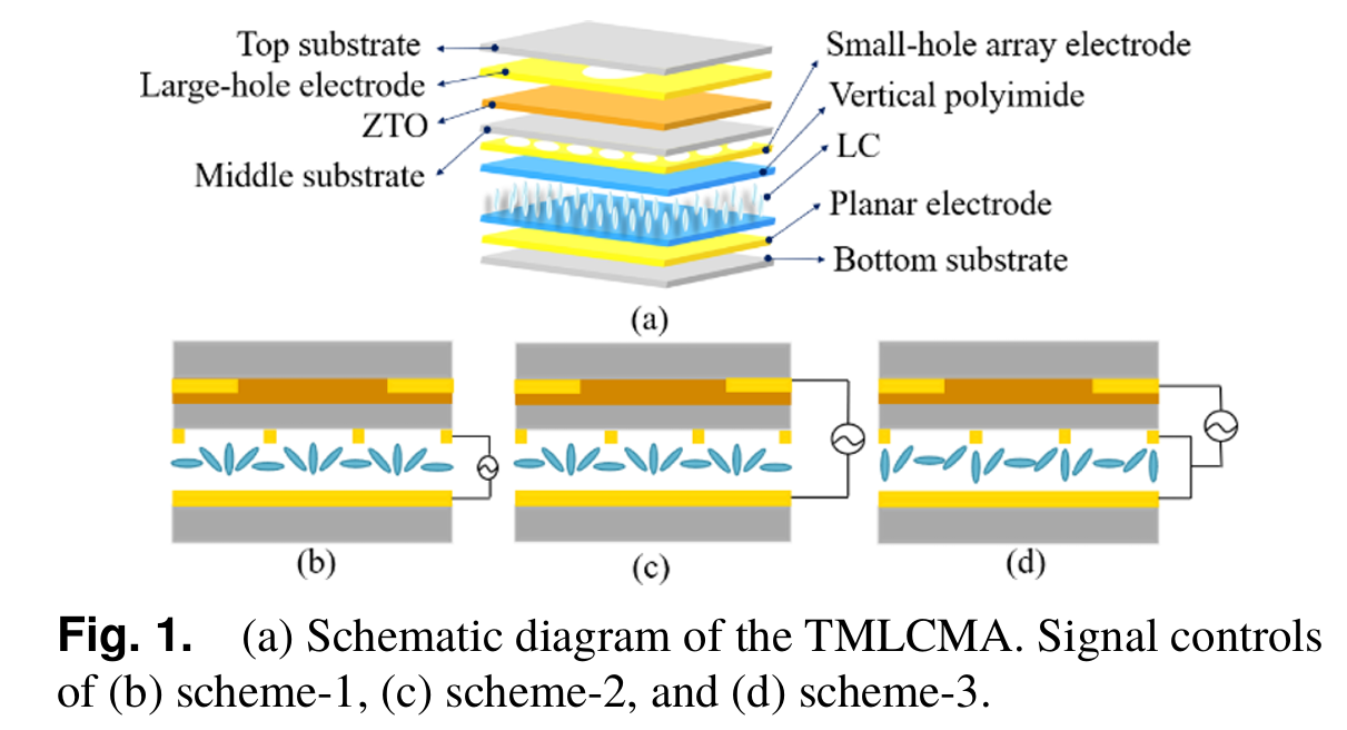
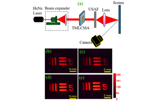
Process製程 & Device Engineer (Research) - Liquid Crystal & Photonics Lab, NCUE國立彰化師範大學 液晶與光電實驗室
Mar 2023 - Jan 2026
National Changhua University of Education國立彰化師範大學02
Research role / project title研究角色 / 專案名稱
Research & Engineering Projects
Selected work精選專案
Research Projects研究專案
Selected process and device work with measurable outcomes.


Recognition
Publications & International Conferences學術論文與國際會議發表
Peer-reviewed publication and conference recognition.
2026
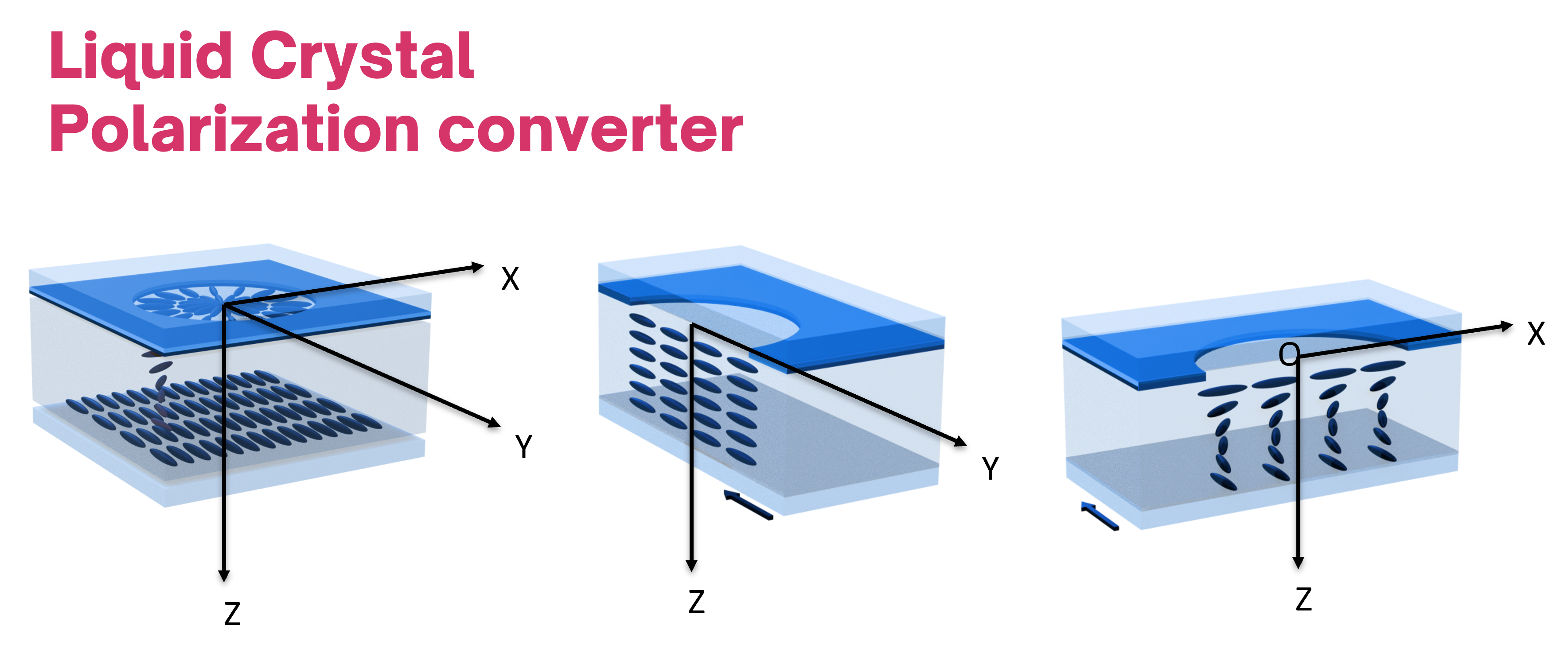
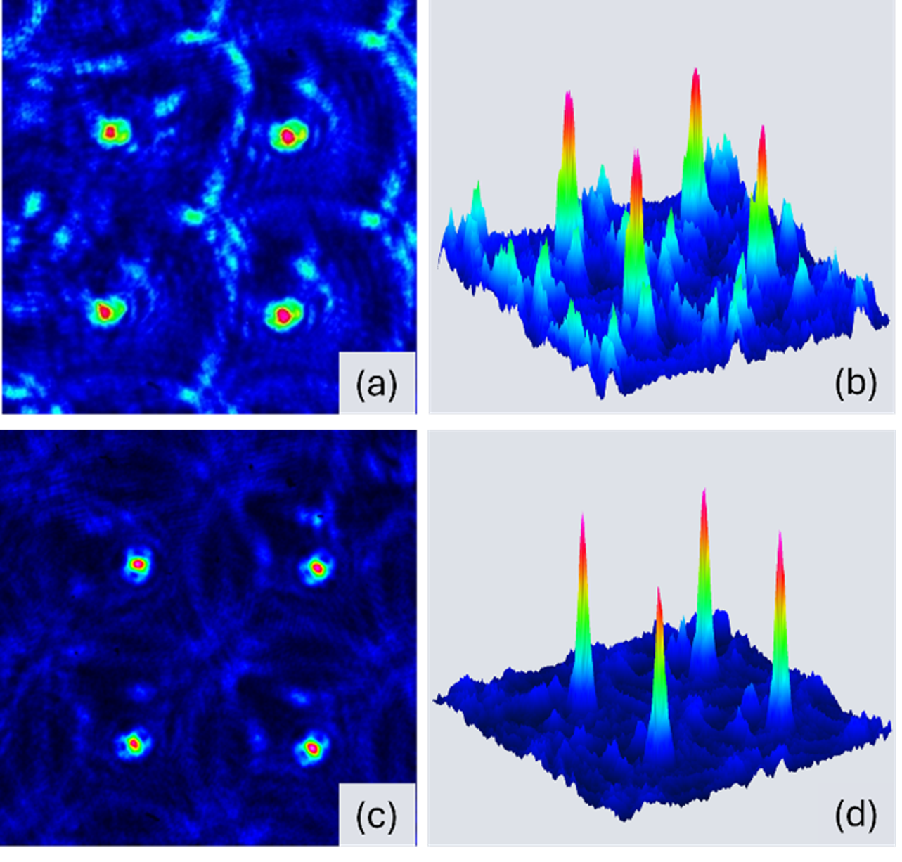
Liquid Crystal Polarization converter Array integrating Vector Vortex Beam Generation整合向量光渦旋產生之液晶偏振轉換陣列
2025
Optics光學 Letters peer-reviewed publication
2024
IDW '24 Outstanding Poster Paper Award獲獎
2023
Taiwan Liquid Crystal Society poster presentation台灣液晶學會海報發表
Certificates & Awards證照與獲獎肯定
Official letters, awards, and certificates.官方經歷證明、獲獎與證書
 View
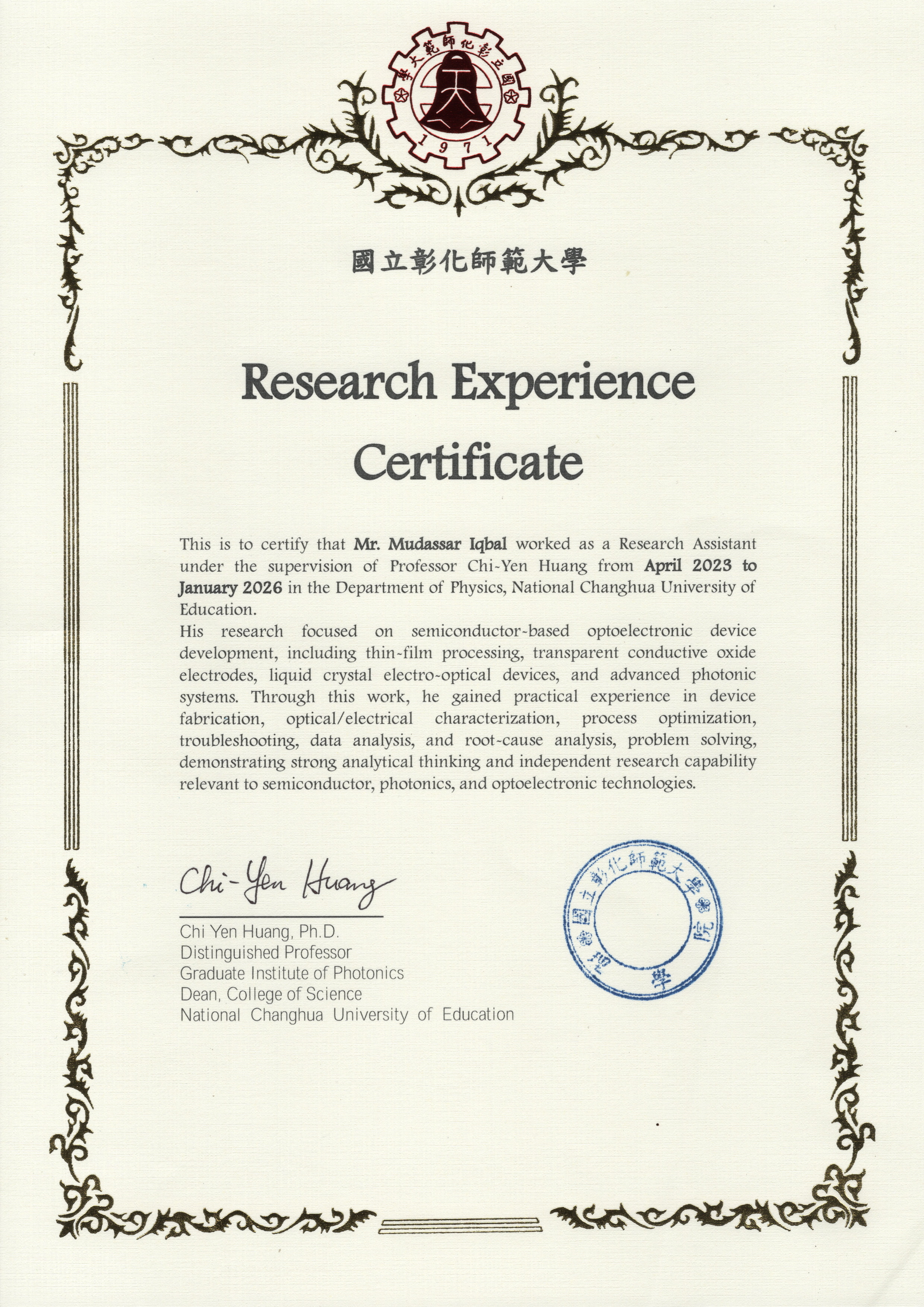
ViewResearch Assistant - Experience Letter研究助理經歷證明
Open document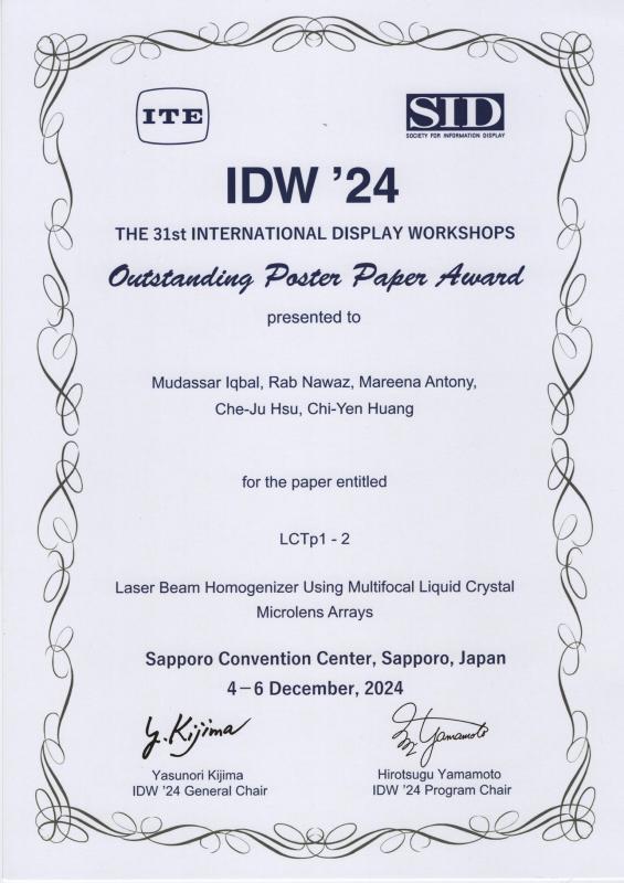 View
ViewIDW '24 Outstanding Poster Paper Award獲獎
Open documentContact
Open to process engineering roles尋求製程工程師相關職位
Seeking semiconductor, photonics, and advanced manufacturing roles where thin-film process development, wet etch, device integration, metrology, and root-cause analysis are valued.
Contact details
LinkedInlinkedin.com/in/raimudassar
LocationChanghua, Taiwan台灣彰化
Adress地址No 1 Jinde Road, NCUE500 彰化市進德路1號 國立彰化師範大學
Target roles目標職位Download CV
Process EngineerThin-Film Process EngineerEtch Process EngineerDisplay/Photonics Process EngineerDevice Integration Engineer